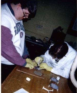
Preparation | Cell Creation ProcedurePreparationCollect all of the materials, read procedure, and mentally prepare for project. It is imperative that one understands all of the procedure before starting. Once one has realized and understood all requirements including temperature and time limitations, and is able to accommodate these requirements, one may begin processing the cells by beginning the process with the hydrofluoric acid cleaning step. (Safety Concerns: General lab procedure will need to be augmented with lab coats, gloves, facial shields, and at least one person should be ready at all times to activate emergency safety procedure, i.e. alerting medical technicians, etc., in case of accident.)
Cleaning the Wafers with HFThis step requires:
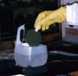
Also, because of the danger of the acid, this process needs to be carried out in a fume hood. Place enough hydrofluoric acid in a plastic container so that the cells will be covered when dipped. Each wafer should be dipped individually into the container for 35 seconds using two plastic tweezers and two hands holding the tweezers. Move the tweezers one at a time so all of the wafer is cleaned. Repeat for all wafers. Finally, each wafer needs to be dried off with whatever relatively inert gas you happen to have lying around your science department. When the step is completed, the cells should have a somewhat cleaner appearance than before. This step can be omitted for experimentation purposes.
Phosphorus DopingThis step requires:
Using a squeegee, paint the phosphorus dopant on the shiny side of the silicon wafer, which shall be designated as the front side. The silicon wafers should be placed onto the tripods and into the kiln, phosphorus side up, using a long tong-like device. The wafers are to remain in the kiln for at least 30 minutes, at about 850°C. At the end of this time, the temperature must be raised to 950°C. Do not heat it too hot, otherwise your wafers may break. Remove the cells from the kiln and allow them to cool. Once the cells are at room temperature, you may proceed with hydrofluoric acid treatment again. Lower the wafers into the acid in the same manner, for 35 seconds. Then, lower them into deionized water before drying them off with a relatively inert gas. The hydrofluoric acid, when finished, can be reacted with sodium hydroxide for disposal. It is worth noting that the phosphorus dopant has a rather noxious smell, and exposure to the dopant should be limited. The cells at this point, along with the tripods, are extremely brittle, and more importantly, extremely hot. One needs to use great care when dealing with the cells at the end of this step.
Anti-Reflective Application (TiO2)This step requires:
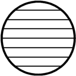
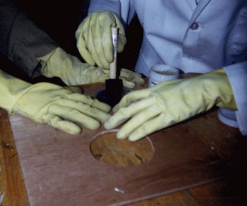
The stencil should be held down on top of the wafer, and titanium dioxide paste applied on top of the dopant layer. The stencil's pattern is opposite that of the silver metallization in the next step. Once this is done, place the silicon wafer on the tripod and inside the kiln, and heat it at 475-550°C for between 1 and 5 minutes. After it is fired, the silicon wafer will be removed from the kiln and cooled down quickly. The front surface should have a bluish tint. After stencilling six to ten cells, the stencil is somewhat easy to break. Since it is very difficult to create a new stencil, requiring great precision and care for several hours, it is necessary to be extremely careful when using the stencil. Also, be alerted that the titanium dioxide will burst into flame at some time in the kiln. This is perfectly normal and not dangerous.
Front Side Metallization (Ag)This step requires:
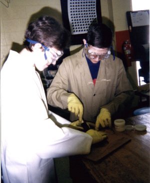
First, use the line stencil to put silver paste on the top of the cell, directly opposite the antireflective coating lines. Then, heat at 120°C for 20 minutes. Next, use the parenthesis stencil to place connecting curves on top of the cell, at both ends of the silver lines. Heat again for 20 minutes at 120°C, and then move directly on to the next step. Take great care when placing the antireflective and front side lines. Note which way the stencils must be placed to create silver lines exactly where the antireflective is not. Greater precision here creates more efficient cells. Also, be sure to wear latex gloves and lab coats during this step.
Back Side Metallization (Ag-Al)This step requires:
After applying the paste, place the cell bottom-side up in the tripod and heat it for 20 minutes at 120°C. Following this, heat needs to be applied at 720-820°C for 30 seconds. Finally, the cells are to be cooled to room temperature.
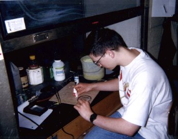
SolderingBecause of the special metals on the cell, silver solder and special flux must be used. The copper wires must be flattened to assist attachment to the cell. One wire is soldered to the top of the cell at a junction point of a parenthesis and a line. The other is soldered anywhere on the back metal. Soldering these cells can be a very difficult skill to master, and one may need to practice using extra materials, or make attempts on earlier cells. The back side soldering is especially difficult, as the wire may fall off easily. Because of this, electrical tape may be used to help secure the solder, although some metal may be torn up if the tape is removed.
|

